Empowering innovation through advanced 2D materials.
Smena Sense develops advanced 2D materials for gas sensing and photonics while engineering precise hybrid nanopores for biosensing and molecular analysis.
Applications
Technology Applications & Benefits
NO2 gas sensing
Our MoS₂-based material enables the development of advanced NO₂ chemo-resistive gas sensors characterized by high sensitivity (ppb), humidity resistance, and strong selectivity towards NO₂. It also detects CH₄, H₂, and NH₄ at ppm levels, making it suitable for environmental monitoring, industrial control, and safety systems.

Production of Ws2 nanopores
Ultra-sharp materials for nano-photonics
Our ultra-sharp 2D materials are applicable in fields such as nanophotonics, extreme ultraviolet (EUV) lithography, and X-ray imaging. Their dimensional precision and optical characteristics support the development of components for high-resolution imaging and light manipulation at the nanoscale.

Production of EBL calibration marks
Our materials are used in the production of calibration marks for electron beam lithography (EBL), ensuring alignment precision and reproducibility in nanoscale fabrication processes. These marks are applicable in research and manufacturing environments where high patterning accuracy is required.
Products
Our material can be used in many distinctly different ways. Take a look at our product list.
- Production of MoS₂ Ink for Gas Sensing
- Fabrication of WS₂ Nanopores
- Production of Ultra-Sharp 2D Materials
- EBL Calibration Marks
- Cleanroom Process Consultancy
1. MoS2 Ink for Gas Sensing
Product description
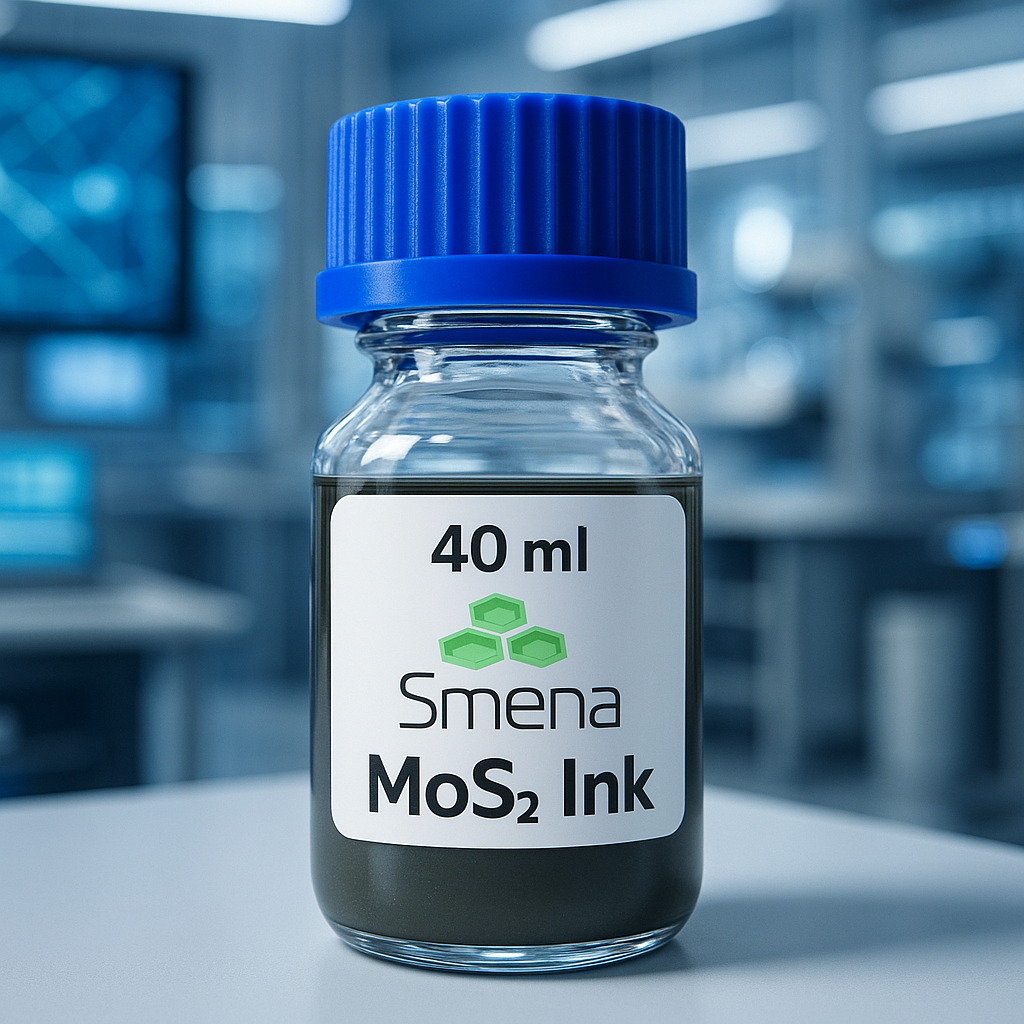
Formulated for high-performance NO₂ detection, our MoS₂ ink offers exceptional sensitivity (ppb-level), strong selectivity, and humidity resistance, making it suitable for integration into Metal-Oxide Semiconductor (MOS) gas sensors.
Specifications: Activated MoS2 flakes distributed in the IPA solution. Distribution solution and the flake sizes can be customized upon request. Standard ink solution includes ~5-10 μm flakes. Ink solution concentration can be customized.


Pricing
Contact us for a quotation for a customized ink that suits your specific needs.
Interested and want to discuss pricing?
2. Hybrid Nanopores
Product description
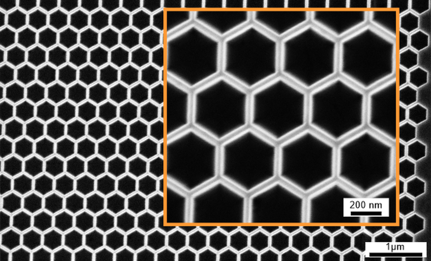
We create hybrid nanopores with atomically sharp triangular and hexagonal shapes. Both single pores and arrays are available, with high reproducibility. Built on WS₂ membranes, they offer excellent stability and precision. Ideal for ionic current measurements and molecular-scale analysis.
Specifcations: Single and arrays of nanopores on 5-10 nm MoS2 and WS2 membrane with a variety of diameters from 1-500 nm with atomically sharp edges. Diameter sizes and pitches can be designed according to the customer’s needs.


Technical specification
Size Distribution: a few hundred nm up to several um scale
Pricing
The price will depend on a range of parameters, please contact us to know more. At present, we can deliver small sample batches, scaling up is a prioroty so keep updated.
Interested and want to discuss pricing?
3. Ultra-Sharp 2D Materials
Product description
We produce ultra-sharp 2D material edges suitable for nanophotonics, EUV lithography, and X-ray imaging applications, where high edge definition and optical precision are required.
Specifications: Atomically sharp channels and grating structures transferred on the desired substrates. Potential substrates include Silicon (Si), silicon dioxide (SiO2), silicon nitride (SiN), hexagonal boron nitride (hBN), Lithium niobate (LiNbO3), Silicon Carbide (SiC), or any other TMD materials. Depending on the customer design and the substrate, we can produce 100´100 um structures in lateral dimensions.


Pricing
The price will depend on a range of parameters, please contact us to know more. At present, we can deliver small sample batches, scaling up is a priority so keep updated.
Interested and want to discuss pricing?
4. EBL Calibration Marks
Product description
Our precision-manufactured calibration marks are designed for electron beam lithography systems, enhancing alignment accuracy and repeatability in nanoscale patterning processes.
Specifications: Ultrasharp edges on the calibration marks to determine the beam size and accurately calibrate the calibration. These calibration marks are fabricated on the desired substrate to reach the desired contrast.


Pricing
The price will depend on a range of parameters, please contact us to know more. At present, we can deliver small sample batches, scaling up is a priority so keep updated.
Interested and want to discuss pricing?
5. Cleanroom Process Consultancy
Service description
Specifications: Expert services for various cleanroom processes.
- High-quality thin film coatings on Silicon or any desired substrate
- Coating materials can be SiO 2 , SiN, Au, Ni, Ti, Cr, Ag
- Electron beam lithography (EBL)
- help designing and nanofabricating sub-15 nm structures on the desired substrate.
- exposures up to 8-inch wafers or fabricate them on small chips.
- Transfer desired patterns to various substrates
- dry etching process to pattern substrates such as Si, SiO 2, and SiC.
- nanostructure fabrication and dry etching of SiC.


Pricing
Every consultancy is priced individually, based on the project complexity.
Interested and want to discuss pricing?
Research & Development
Our work is based on several scientific publications
Everything we do at Smena is solidly based in science. Our founder Timur Shegai is a world class physicist (having published as last author in Nature magazine on the topic of light-matter interaction) and is actively involved in everything we do. You can trust that the knowledge built in his research group at Chalmers University of Sweden is part of any delivery from Smena.
We at Smena strive for a green development
Sustainability, a big word. At Smena this means we think several hundred years ahead. Only then can human activity be truly sustainable. Honestly, almost nothing we humans do presently can be seen as truly sustainable. You can trust that Smena is doing our utmost to think really long term, and taking care of both ourselves and our planet.
We use a scalable resource
MoS2 can be found in nature as a relatively abundant mineral – molybdenite, which is an infinitely scalable resource. MoS2 is a semiconducting 2D analog of famous graphene.
It is believed that thanks to the remarkable physical, chemical, optical and mechanical properties, the material will find use in future industries.


About
Built on Research, Driven by Impact
Smena Sense is an academic spin-off from Chalmers University of Technology, focused on developing advanced 2D materials for applications in gas sensing, nanophotonics, and biosensing. As a material-based company, we combine scientific expertise with a commitment to practical innovation, delivering high-performance solutions that enable next-generation technologies. Sustainability is a core value in our research and development process, guiding our approach to responsible materials engineering and long-term impact.
Smena is based in Gothenburg, Sweden and is working with the principles of self management and self organisation described the colour teal. Our ”why” will always be more important than the ”what”.
Our team

CEO
Patrik Bjöörn

Business Coach
Ana Maria Popescu

Professor & co-founder
Timur Shegai

Business Developer
Jakub Janczak

Research Engineer
Betül Küçüköz

Industrial Post-Doc
Abhay Agrawal
Get in touch
Address
Doctor Forselius Gata 24 1602,
413 26 Gothenburg
Sweden